Industries and Applications
Discover ACM’s Industries and Applications
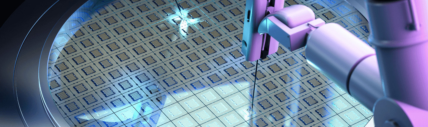
At ACM Research, we focus on developing unique single and batch wet wafer processes to address challenges in IC and compound semiconductor device manufacturing, wafer-level packaging, and wafer manufacturing and reclaim. Our high-performance, cost-effective processes can be customized across a multitude of manufacturing steps to help you improve your productivity and product yield.

IC and Compound Semiconductor Manufacturing
The tools used to manufacture silicon integrated circuits (ICs) and compound semiconductors (also known as III-V materials) are often similar. But the process recipes can be significantly different due to the characteristics of the substrate materials. At ACM Research, we develop unique wafer processes that address challenges in both IC manufacturing and compound semiconductor manufacturing.
Wafer-level Packaging
If you’re following the Heterogeneous Integration Roadmap, you know advanced wafer-level packaging processes are critical to improving the power, performance, area, and cost of next-generation semiconductor devices. From FOWLP and 2.5D interposers to 3D stacks and chiplet architectures, your manufacturing processes will benefit from our wafer-processing expertise, customized to your requirements.
Wafer Manufacturing and Reclaim
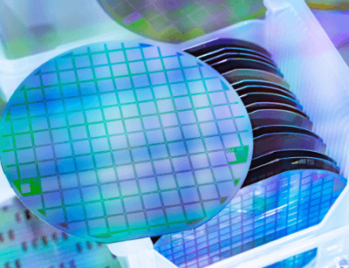
Device manufacturing begins with manufacturing the wafers in a five-step process. Wafers are sliced from an ingot wafer, polished to a desired thickness, chemically etched to remove mechanical damage, polished using chemical mechanical planarization (CMP), and cleaned and inspected to ensure quality. Our wet bench and SAPS tools are ideal for performing all your wet processes used in wafer manufacturing, including etch, CMP, and cleans.

Contact Us
Looking for customized solutions for IC and compound semiconductor manufacturing, wafer-level packaging, and wafer manufacturing and reclaim?