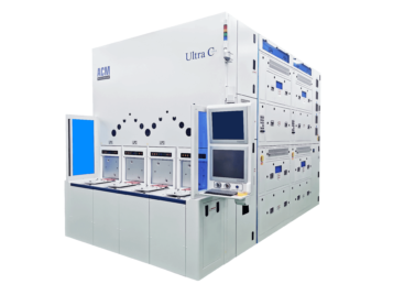
Cleaning Systems—Ultra C b
For contactless backside cleaning
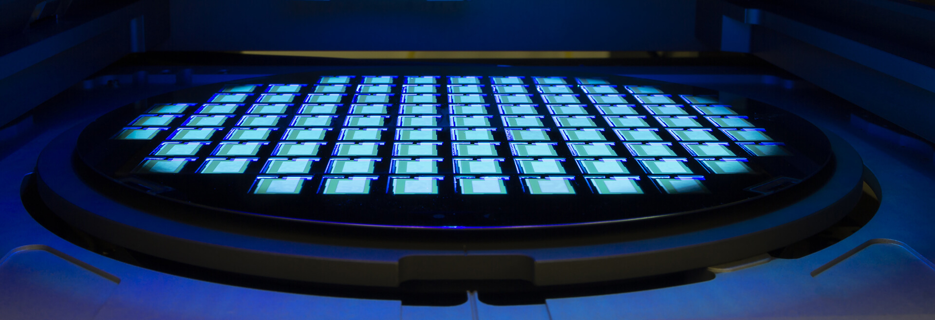
The Ultra C b backside cleaning tool from ACM Research is designed for 200mm or 300mm wafers’ backside clean or etch processes widely used in IC wafer manufacturing, wafer level packaging and the power device industry. It uses a contactless Bernoulli wafer chuck to prevent the frontside of the wafer from damage. When chemical solutions are dispensed onto the wafer backside, the device side is protected from chemical solutions or vapors via nitrogen (N2) gas delivered from the Bernoulli chuck.
The Ultra C b system delivers effective particle performance and etch uniformity, while meeting undercut requirements on the wafer bevel and pin mark-free control. This proprietary design allows the Ultra C b to be customized for throughput exceeding 300 wph for applications with short chemical process times. The flexible etching process can accommodate either silicon etch or film removal, and the system delivers precise control of chemical and etching uniformity. In addition, the Ultra C b can handle a variety of substrates, such as heavily doped wafers, bonded wafers and ultra-thin wafers. The Bernoulli chuck can handle ultra-thin wafers or Taiko wafers with high warpage. An optional advanced non-contact robot can be added to aid in handling ultra-thin or Taiko wafers.
Features & Specifications
- Up to eight cleaning chambers
- Wafer-flipping function
- Multiple chemicals for:
- HF solution for silicon dioxide etching
- RCA solutions for backside clean
- HNO3/HF solution for backside etching process
- Poly/SiN films removal
- Silicon etchants for silicon etching, back-side thinning or through-silicon via (TSV) reveal

Contact Us
Looking for spare parts and customer support for your ACM Research Systems?