Cleaning Systems—Ultra C SAPS
For cleaning flat and patterned wafers at advanced technology nodes
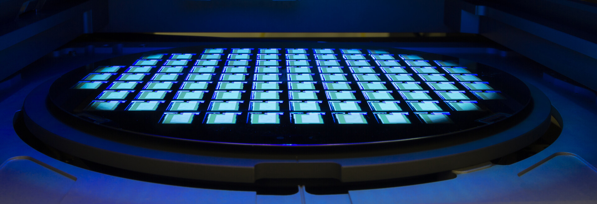
SAPS™ – advanced wafer cleaning technology
ACM’s patented Space Alternated Phase Shift (SAPS™) technology employs alternating phases of megasonic waves in the gap between a megasonic transducer and the wafer. Unlike the stationary megasonic transducers used in previous generations of megasonic wafer cleaning systems, SAPS technology moves or tilts the transducer while the wafer rotates, enabling megasonic energy to be delivered uniformly across all points on the wafer, even if the wafer is warped. On a microscopic level, this megasonic energy is able to reach every point on the wafer surface, to remove random defects much more effectively and completely than conventional megasonic or jet spray processes. Radicals for removing the random defects are generated in dilute chemical solution by the megasonic energy. The mechanical force of cavitations generated by megasonic energy enhances the mass transfer rate of dislodged random defects and improves particle removal efficiency. SAPS can accomplish all of this in less time than conventional megasonic cleaning products, without loss of material and without roughing wafer surfaces.
SAPS technology has demonstrated its advanced wafer cleaning capabilities as nodes shrink from 45nm to 10nm and even beyond, for which jet spray technology is not effective. Moreover, users of SAPS equipment have already expanded their application of ACM tools, adding cleaning to more steps in the manufacturing process to increase wafer yields.
Smart Megasonix™
Outperforming conventional megasonics
Traditional megasonic wafer cleaning has reached its limits. The conventional cleaning methods are no longer able to remove the smallest killer defects without causing device damage. This is why ACM has developed Smart Megasonix™—a smarter, more innovative suite of single wafer wet cleaning technologies that can be used at existing and future process nodes across the range of processing steps—to achieve more thorough, comprehensive cleaning without damage to device features. These proprietary ACM technologies are able to control both the power intensity and the distribution of megasonic cleaning—to achieve dramatically positive results.
SAPS wafer cleaning applications
- Post CMP
- Post Hard Mask Deposition: As part of the photolithographic patterning process, hard masks have been developed to etch high-aspect-ratio features of advanced chips that traditional masks cannot tolerate. SAPS cleaning technology can be employed following each deposition step involving hard masks that use nitride, oxide or carbon-based materials to achieve higher etch selectivity and resolution.
- Interconnects and Barrier Metals: SAPS technology can improve the removal of residues and other random defects from interconnects with deep contacts or vias during the chip fabrication process:
- Post-Contact/Via Etch: Etching processes are commonly used to create patterns of high-density contacts and vias. SAPS technology can be applied after each such etching process to remove random defects that could otherwise lead to electrical shorts.
- Pre-Barrier Metal Deposition: Copper wiring requires metal diffusion barriers at the top of via holes to prevent electrical migration during operations leading to leakage or opens. SAPS technology can be applied prior to deposition of barrier metal to remove residual oxidized copper, which otherwise would adhere poorly to the barrier and impair performance.
- High-Aspect-Ratio Structure Clean: SAPS technology provides uniform megasonic energy distribution to the wafer surface and has a significant capability for residue removal in structures with high aspect ratio, such as through silicon via (TSV), deep trench and deep via with aspect ratio larger than 10:1.
- Recycled Test Wafers: Manufacturers routinely process wafers through a limited portion of the fabrication steps in order to evaluate the health as well as use wafers for non-product purposes such as inline monitoring. These wafers used for purposes other than manufacturing revenue products are known as test wafers, and manufacturers seek to re-use a test wafer for more than one test. As test wafers are recycled, SAPS technology can be applied to reduce random defect levels of a recycled wafer.
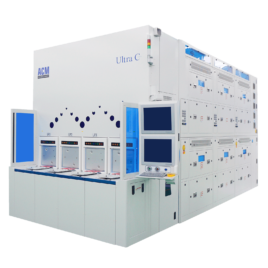
SAPS Systems
ACM currently offers three models of wafer cleaning systems based on our SAPS technology: The SAPS II, SAPS V and SAPS VI are single wafer, serial-processing tools that can be configured to customer specifications. With appropriate dilute chemicals they can be used to remove random defects from wafer surfaces or interconnects and barrier metals in front-end chip fabrication or for recycling test wafers. Combining ACM’s advanced megasonic and chemical cleaning technologies, these tools remove random defects with greater effectiveness and efficiency than conventional wafer cleaning processes. They also enhance process flexibility and reduce chemical consumption.
SAPS II
This is our most commonly used machine. With a total of 8 single wafer cleaning chambers, this model is well suited for all parts of the front end manufacturing process
SAPS V
This is the largest ACM SAPS tool. With 12 single-wafer cleaning chambers, this tool is able to hold and use multiple chemicals, which helps increase the throughput and efficiency of the cleaning process.
SAPS II Features & Specifications
- Up to 8 chambers, throughput up to 225 wafers/hour
- Double-sided cleaning capability, up to 5 cleaning chemicals for process flexibility
- 2-chemical recycling capability to reduce chemical consumption
- Imaging wafer detection to reduce wafer breakage
- Chemical delivery module delivers dilute hydrofluoric acid, RCA SC-1 solution, functional de-ionized water and carbon dioxide to each chamber
- Compact size: 2.35m x 45.53m x 2.85m (WxDxH)
SAPS V Features & Specifications
- All SAPS II features, plus the following:
- Up to 12 chambers, throughput up to 375 wafers/hour
- Chemical supply system integrated into mainframe
- Inline mixing method replaces tank auto-changing, reducing process time
- Enhanced drying technology using hot isopropyl alcohol and de-ionized water
- Compact size: 2.35m x 6.7m x 2.85m (WxDxH)
SAPS VI Features & Specifications
- Up to 18 chambers, throughput up to 800 wafers/hour
- Double-sided cleaning, with up to 5 cleaning chemicals in each system
- Example: DHF, DSP+, f-DIW, FOM, SC1, SC2, DIO3, ST250, EKC580, NE111, IPA and other formulated solutions
- 2-Chemical reclaim, low tool COO
- Optional enhanced drying technology with room temperature IPA or hot IPA
- Optional dual-fluid N2-DIW spray or N2-SC1 spray assist particle removal
- Optional ACM patented SAPS Megasonic assist flat and via particle removal
- Optional ACM patented TEBO megasonic for high efficiency pattern damage free clean
- Compact Size: VI 2.35m×6.30m×2.85m (W×D×H)

Contact Us
Looking for spare parts and customer support for your ACM Research Systems?