
Wafer-Level Packaging
Discover How We Support Wafer-level Packaging
If you’re following the Heterogeneous Integration Roadmap, you know advanced wafer-level packaging processes are critical to improving the power, performance, area, and cost of next-generation semiconductor devices. From FOWLP and 2.5D interposers to 3D stacks and chiplet architectures, your manufacturing processes will benefit from our wafer processing expertise, customized to your requirements.
Do You Have Varied Needs for Your WLP Processes?
Our WLP offering extends beyond our leading-edge cleaning systems to support a broad spectrum of advanced WLP applications. We’ve leveraged our proprietary wet processing technology and expertise into a range of customized single-wafer tools to suit your back-end wafer assembly and packaging needs.
- Our fully automated Coater features a unique auto-clean module for ease of use
- Our flexible Developer performs three different photoresist developing methods
- Our efficient Stripper integrates batch and single-wafer processing into one system
- Our high-speed ECP plating system supports critical WLP plating steps including pillar, bump, and RDL
Because diversity is the name of the game for WLP, we accommodate your special requests and deliver custom-made, differentiated equipment that integrates multiple ACM technologies to enhance performance at a competitive price.
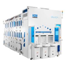
Plating Systems—Ultra ECP ap
Learn More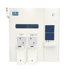
Coater Systems—Ultra C ct
Learn More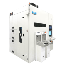
Developer Systems—Ultra C dv
Learn More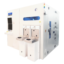
Wet Etching Systems—Ultra C we
Learn More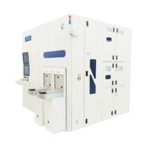
Wet Stripping Systems—Ultra C pr
Learn More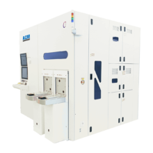
Cleaning Systems—Metal Lift Off
Learn More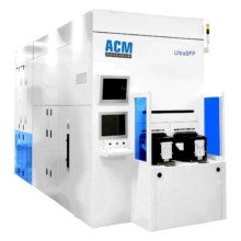
Stress Free Polishing Systems—Ultra SFP
Learn More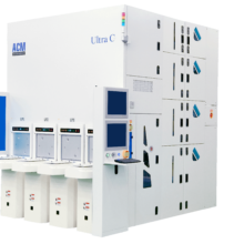
Scrubber Systems—Ultra C s
Learn More
Contact Us
Looking for customized solutions for your wafer-level packaging processes?
